
Technology Dimension Overview
FUTUR-IC seeks to develop materials and component technology for high-performance resource-efficient microchip systems.
Electronic-photonic Integration
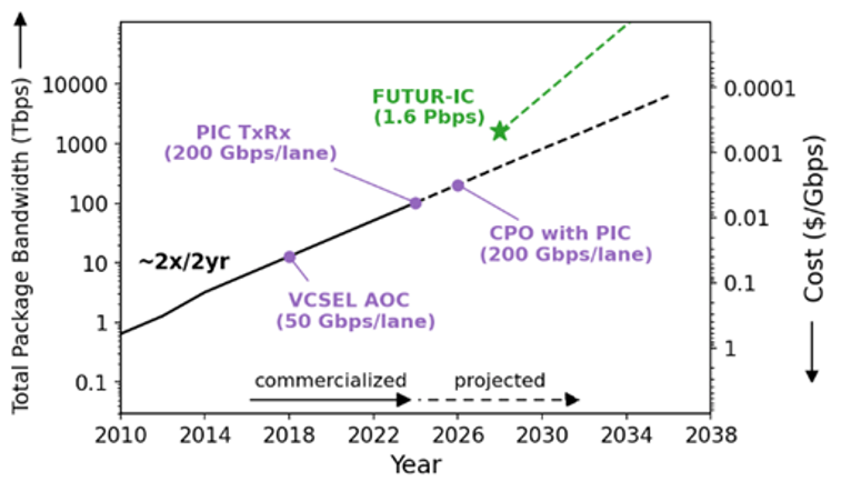
The traditional dimensional scaling of microchip feature sizes that has maintained increases in number of transistors per chip and economies of scale in production over the last 40 years, is migrating to a new metric, an increase in the number of chips per package. FUTUR-IC is trailblazing a resource-efficient, performance scaling path with package-level electronic-photonic integration, that leapfrogs over the current technology barriers to scaling function and speed. FUTUR-IC targets more than a two generation advance for lower cost manufacturing and a total package bandwidth of ~10 petabits per second by 2030 instead of 2038. The FUTUR-IC prototypes have demonstrated (i) a flip-chip optical interconnect, (ii) an integrated, multilevel micro-reflector connector, and (iii) an optical fiber connector assembly. The first two innovations, patented by MIT, enable large bandwidths with lower energy and cost per transmitted bit. The connector assembly from Tyndall National Institute, Ireland, is the testbed platform for technology transfer of FUTUR-IC packaging solutions in partnership with the semiconductor industry.
Advances in waveguide to waveguide couplers for 3D integrated photonic packaging
In this paper, MIT researchers provide an overview and comparison of devices used for optical waveguide-to-waveguide coupling including inter-chip edge couplers, grating couplers, free form couplers, evanescent couplers, cantilever couplers, and optical wirebonds. In addition, technology for efficient transmission of light through chips is discussed including guided mode and free form photonic vias for substrates including silicon, glass, and organics. The results are discussed in the context of potential applications including co-packaged optics switch packages, replaceable biochemical sensors, optically connected memory, optical computing, integrated quantum photonics, and integrated LiDAR systems to show possible improvements in energy efficiency, performance, and cost.
PFAS Chemistries
PFAS and its implications for the semiconductor industry was hosted by MIT.nano, Edwards Vacuum, the Initiative for Knowledge & Innovation in Manufacturing at MIT (IKIM), and FUTUR-IC. Talk by Chris Jones, Environmental Solutions Business Development Manager, Edwards Vacuum, with introduction by Anu Agarwal, Principal Research Scientist, Microphotonics Center and Materials Research Laboratory.
PFAS present a complex challenge for semiconductor manufacturing: they are essential for high-performance processes but are increasingly under regulatory scrutiny due to persistence and toxicity.
Edwards Vacuum is addressing this through a dual approach of awareness and action. On awareness, they are collaborating across the industry (including IKIM and FUTUR-IC) to map PFAS usage, trace environmental pathways, and communicate risks. On action, they are testing vacuum and abatement systems, measuring destruction and removal efficiencies (DREs) for gases such as CF₄, C₃F₈, and C₄F₈, and assessing whether combustion treatment could generate PFAS. Additional studies include longer-chain species and plasma simulations of chamber conditions.
They are also analyzing residues from returned vacuum pumps to identify real-world PFAS formation pathways. Alongside this, Edwards is auditing designs, working with suppliers, and pursuing substitution strategies, with a goal of reducing or eliminating PFAS in new equipment by 2030.
View the presentation here: PFAS in Semiconductors: From Awareness to Action.
Resources

GenTronics Phone Supply Chain Game

Advances in waveguide to waveguide couplers for 3D integrated photonic packaging

Graded index couplers for next generation chip-to-chip andfiber-to-chip photonic packaging

High density vertical optical interconnects for passive assembly

Hands-On Photonic Education Kits: empowering the integrated photonics workforce through practical training
