
FUTUR-IC hosts advanced semiconductor packaging bootcamp
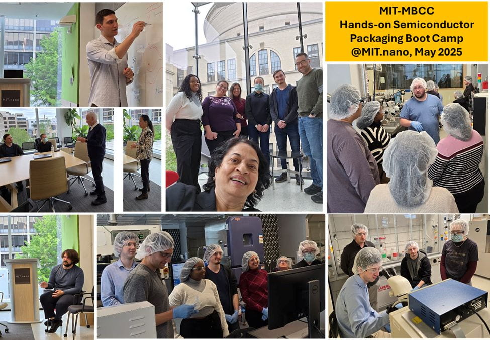
This week Massachusetts Institute of Technology’s FUTUR-IC team had the pleasure of hosting five students from Massachusetts Bay Community College: Iciss Cato, Inas Dawoud, Gena Megelly, Orion Melanson, and Gwyneth R.-Smith.
The students were here to learn about advanced semiconductor packaging through a hands-on boot camp, which is a part of NCAIST, an NSF-ATE program (PI: Prof. Abraham Michelen SUNY-Poly, Albany; MA PI: Prof. Marina Bograd, MassBay Community College; MIT PI: Anuradha Agarwal).
Boot camp attendees were trained to operate three packaging tools in the LEAP (Lab for Education and Application Prototypes) at MIT.nano: Die Saw, Wire Bonder and Die Bonder. Hands-on training was provided by a team of staff and students from MIT’s DMSE and Materials Research Laboratory, Dr. Drew Weninger and Dr. Luigi Ranno, as well as staff from MIT.nano, Kristofor Payer, Justin Pellegrine, Benjamin Newcomb, and Cody Corey. The training was supplemented by Virtual Reality (VR) simulations of (1) photonic devices such as waveguides, bends, and escalators and (2) packaging tools such as the Die Saw and Die Bonder. To learn about resource-efficient manufacturing in the semiconductor industry, attendees also had access to a Game called “Gentronics” in which they were “owners” of a cellphone factory, during which they had to maximize profits and performance while minimizing use of resources like minerals, water, chemicals, plastics, and other materials. These VR simulations and game were created by the MIT IKIM’s (Initiative for Knowledge and Innovation in Manufacturing) Virtual Manufacturing Lab team of Dr. Sajan Saini, Ira Fay, Trevor Morrisey, and Jaymie Krambeck.
At the end of each day, boot camp attendees reflected on their learning and engaged with instructors in discussions about electronic-photonic packaging, including conventional electronic packaging techniques, as well as novel cutting-edge electronic-photonic packaging ideas (Thank you to Dr. Drew Weninger and Dr. Luigi Ranno for sharing their PhD research).
Of course, the boot camp included a tour by Kristofor Payer of the entire MIT.nano fabrication facility, where attendees learned about several complex steps which are encountered in semiconductor manufacturing: physical and chemical vapor deposition, lithography, plasma etching, packaging, characterization, and imaging. They heard about six-sigma manufacturing from Dr. Pradnya Nagarkar, and requirements across the semiconductor supply chain to maintain vibrant industry growth, from Prof. Lionel Kimerling.
What was most refreshing was attendee enthusiasm and wonder!
Their never-ending questions were a source of inspiration for lively discussions. Thank you to all of them for sharing their time with us and thank you to the MIT team for their dedication to teach and train the next generation!